Welcome:GZTECH
Welcome:GZTECH
2020-2021 is a big year for photovoltaic equipment. In 2020, the demand for battery segment grew rapidly (Tongwei, Longi battery expansion), and in 2021, the demand for silicon wafers grew rapidly (new silicon wafer production expanded), thereby driving the performance of photovoltaic equipment companies to improve, and at the same time promoting the rapid landing of large-scale production, HJT and other new technologies.
Demand side: In 2022, the newly installed photovoltaic capacity is expected to reach 210GW.
Supply side: The silicon material is still profitable. It is expected that the industry will continue to expand production in 2022, and new technology production capacity is expected to usher in an explosion.
Technology side: The wave of technology is approaching, and a segmented market of tens of billions of equipment will be bred, component technologies will flourish, and multiple equipment will benefit together.
A conventional scribing machine uses a pulsed laser to process a cutting line through the surface on the back of the battery, and then uses mechanical methods to split the battery sheet along the cutting line. There are inevitably two disadvantages: one is that the laser thermal ablation process will leave a lot of thermal damage on the cutting surface, which reduces the mechanical strength of the cell; second, for large-size silicon wafers, it is very easy to break. With the birth of ultra-small cell pitch (zero pitch, or even negative pitch), large-size silicon wafers, and ultra-low temperature batteries, conventional laser scribing processes are difficult to meet ultra-high processing quality requirements, and the laser non-destructive splitting of silicon wafers came into being.
Laser non-destructive splitting means that the silicon wafer produces a large temperature gradient through the precise control of laser heating and local auxiliary cooling. The material generates thermal stress to the fracture threshold and fractures, and the crack propagates along the thermal gradient caused by the laser beam path to completely separate the material. The core principle is laser thermal stress-controlled fracture technology. In order to precisely control the direction of the crack, it is necessary to process an ultra-small notch at the beginning and end of the cell, so that the fracture propagation starts from the notch to the end of the notch.
In the development of large-scale, thin-sheet, and high-efficiency battery module technology, laser non-destructive cutting, as a new type of photovoltaic cell cutting technology, has the advantages of size compatibility, no mechanical damage, high efficiency, and less pollution, which is an important link in the promotion and development of large-size cells and high-efficiency modules in the future.
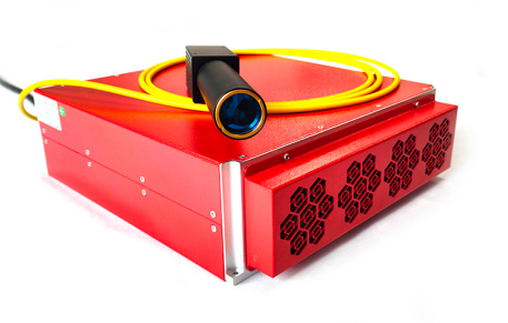
According to the principle of laser non-destructive slitting, GZTECH uses a 70W MOPA laser to draw two 2mm long groove lines on both ends of the silicon wafer, and the depth can reach 40% of the thickness of the silicon wafer. The laser has a wide range of pulse width and frequency, wide adjustable parameters; good beam quality M2<1.5, good focusing characteristics; linear output power adjustment, stable energy, long-term reliable processing; small size, air-cooled structure, and easy to integrate.

YFPN-70-GM
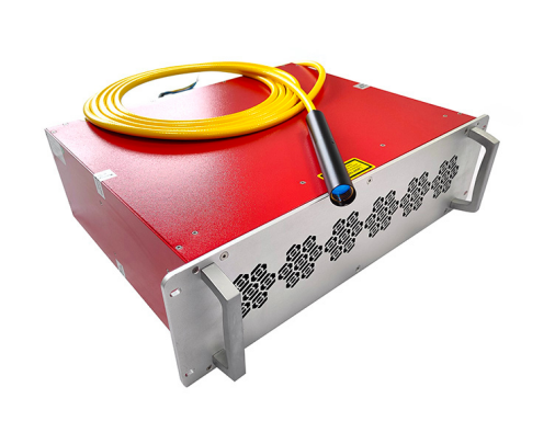
A 300W single-mode continuous laser is used to move along the notch at a high speed of 230mm/s, and the silicon wafer is cracked along the notch under the action of thermal stress. The laser beam quality is good, M2<1.2; compact structure, small size, air-cooled structure; all-fiber, no optical devices, integrated optical path, long-term stability, no maintenance.

YFCW-300-SM
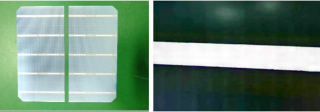
After testing, the silicon wafer has no burr on the surface after non-destructive cutting, with minimal heat-affected zone, smooth and white cross-section, and no damage points.

Test non-destructive scribing effect
GZTECH is a leading supplier of advanced industrial laser products for precision manufacturing. In order to meet the needs of various customers, we are building a layout with Wuhan headquarters as the center and five major offices serving the whole country. At present, there are three major offices in Shenzhen, Suzhou and Jinan, all of which can provide samples for customers. We welcome customers to discuss the development of new laser processes with us.
By continuing to use the site you agree to our privacy policy Terms and Conditions.